A flipflop circuit is a binary cell capable of storing 1 bit information as it can store either 0 or 1 at any time, it can also be called ‘bistable multi-vibrator’. It has two outputs, one for normal value and the other for the complemented value of the bit that is stored in it.
There are varieties of flipflops used in electronic devices. They are described below:
1. RS Flipflop:
It is a basic type of flip-flop constructed using either NOR gates or NAND gates in cross-connected form. The two possible constructions of this type of flipflops are in the following figures. The cross-coupled form shown in the figure constitutes the feedback. This type of flipflop can also be called as direct coupled RS flipflop or SR latch as it doesn’t have any clock input. The R and S represent ‘reset’ and ‘set’ inputs respectively.
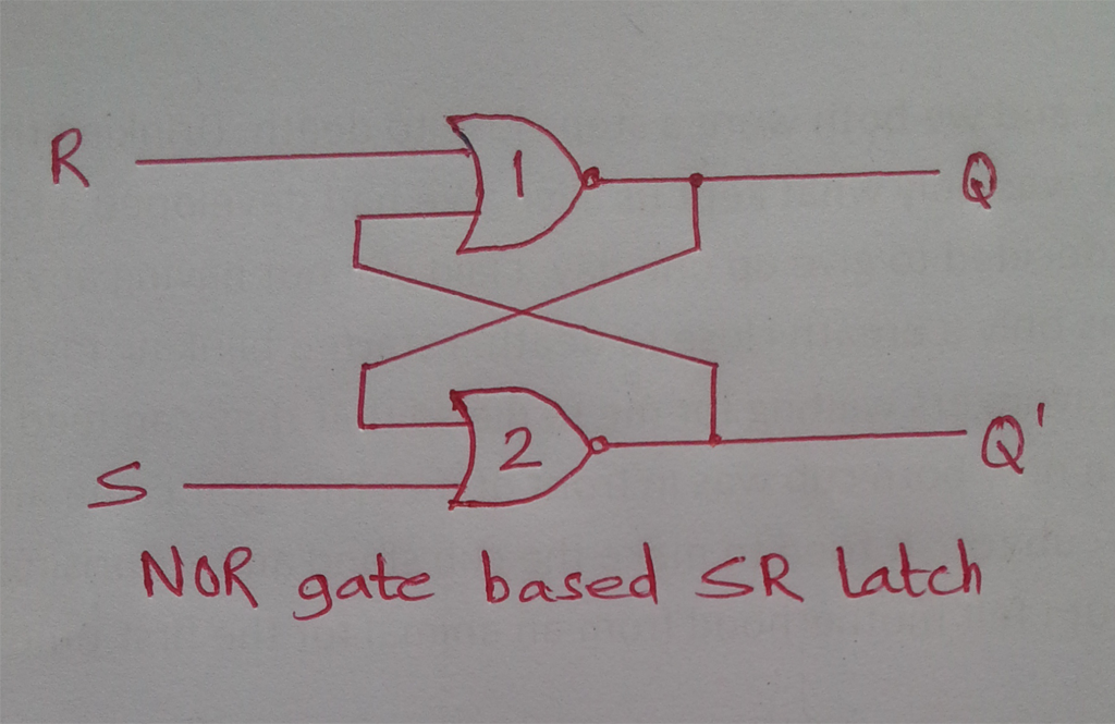 |
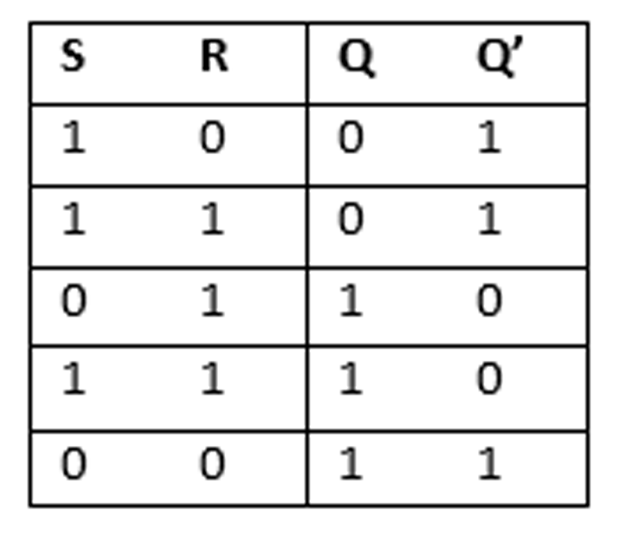
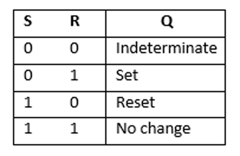
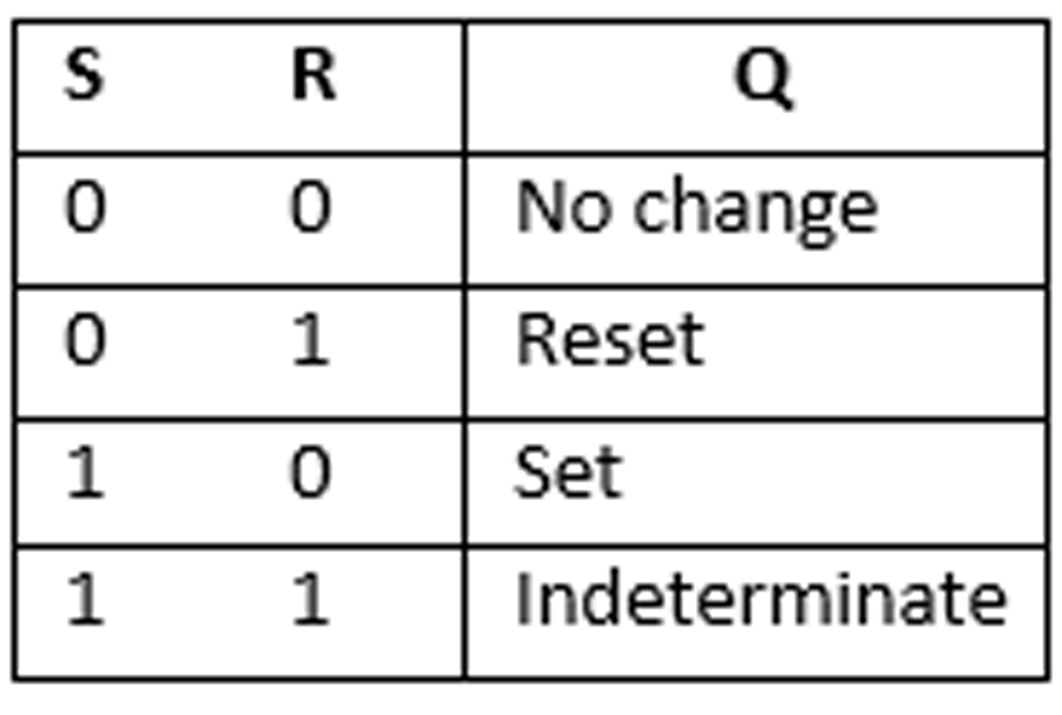 To analyze the operation of the above circuit, we must keep in mind that the output of a NOR gate is 0, if any input is 1 and the output is 1 only when all the inputs are 0. Initially, assume S = 1 and R = 0. Since gate 2 has an input 1, its output Q’ must be 0. Due to this, both inputs of gate 1 are at 0 and hence, Q is 1. When the set input is returned to 0 (S = 0 and R = 0), the output remains the same, as Q is 1, leaving one input of gate to equal to 1. Due to this, Q’ becomes 0 and hence, both the inputs of gate 1 are 0, due to which Q is 1.When 1 is applied to both the set and reset inputs, both Q and Q’ are equal to 0, which violates the fact that the outputs Q and Q’ are the complements of each other. For any flipflop, when Q = 1 and Q’ = 0, it is called to be in ‘set’ state. When Q = 0 and Q’ = 1, it is called ‘reset’ state or ‘clear’.
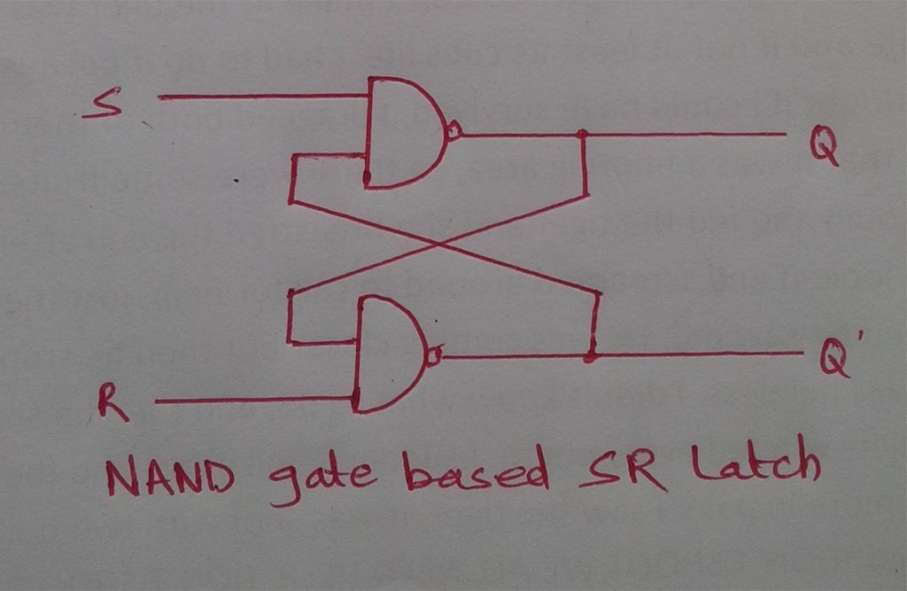 |
The operation is same as that of NOR gate and we should keep in mind that when one of the inputs is 0, the output is 1.
2. Clocked RS Flipflop:
 |

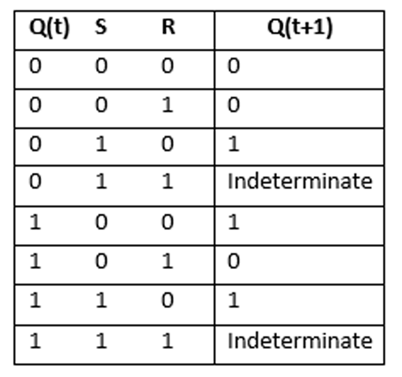
The basic flipflop is an asynchronous circuit. By adding gates to the input of basic circuit, the flipflop can be made to respond to the input levels during the occurrence of a clock pulse. The basic circuit diagram of clocked RS flipflop is shown in the figure given above. As in the figure, the outputs of the two AND gates remain zero as long as CP (Clock Pulse) remains zero, regardless of the S and R input values. When the clock pulse goes to 1, information from the S and R inputs reaches to the basic flipflop. The graphic symbol, as in the figure given above, contains three inputs, S, CP and R. The output of flipflops are marked with Q and Q’. The characteristic table or truth table gives the nature of normal output after the clock pulse is applied. Q is the binary state of flipflop at a given time, referred to as present state and Q(t+1) is the state of the flipflop after the occurrence of a clock pulse and is referred to as next state. The characteristic equation of the flipflop, derived from the k-map, specifies the value of next state as a function of present state and the inputs.
3. D Flipflop:
 |
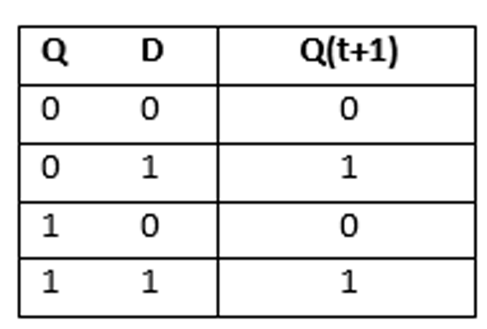 |

The D flipflop is the modification of the clocked RS flipflop. As in the figure given above, D flipflop contains only two inputs, D and CP. The D input goes directly to the S input and its complement to the R input. As long as CP is 0, the 3 and 4 bits have a 1 in their outputs regardless of the value of D input. From the truth table of D flipflop, we can say that the output of D flipflop is same as that of the input D. The D in D flipflop represents its ability to transfer data without any change. It is basically as RS flipflop with an inverter in the R input.
4. JK Flipflop:
 |
 |

A JK flipflop is the modified form of RS flipflop in the sense that the indeterminate state of RS flipflop is defined. The inputs J and K behave like inputs S and R to set and clear the flipflop. When the inputs J and K of the JK flipflop are the same simultaneously and are equal to 1, the flipflop switches to its complement of the current state, i.e. if Q = 1, it changes as Q(t + 1) = 0 and vice versa. The logic diagram of JK flipflop is shown in the figure given above. The Q output is ANDed with K and CP input and Q’ is ANDed with J and CP.
So, according to the characteristic table, the JK flipflop behaves like an RS flipflop except when both J and K are equal to 1. When both J and K are 1, the clock pulse is transmitted through one AND gate only, the one whose input is connected to the flipflop output which is presently equal to 1. Thus, if Q = 1, the output of the upper AND gate becomes 1 and the flipflop is reset. If Q’ = 1, the output of the lower AND gate becomes 1, when J = 1, the flipflop is set. In each case, the output state of the flipflop is complemented. This is called toggling of JK flipflop and is defined only when J = 1 and K = 1. The JK flipflop with inputs J = 1 and K = 1 is said to be in toggle mode.
Note that, in JK flipflop, when a CP signal is equal to 1 while J = K = 1, after the outputs have been complemented once, may cause the repeated and continuous transition of output. This problem is called race condition. To avoid this undesirable operation, the clock pulse must have a time duration which is smaller than propagation delay of the flipflop. The restriction on the pulse width is eliminated with the Master Slave Flipflop.
5. T Flipflop:
 |
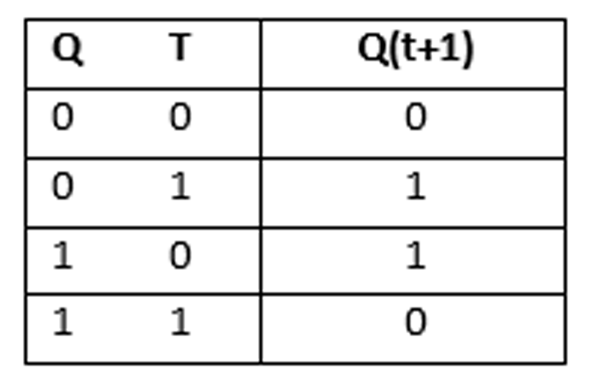 |

The T flipflop is a single input JK flipflop. It is obtained from JK flipflop when J and K inputs are the same. The name ‘T’ comes from the ability of this device to toggle or change the current state when its input is one.
Triggering of Flipflop: The state of a flipflop is switched by the momentary change in input signal. The change in this signal upon which the operation of a flipflop is largely dependent is called a trigger and the process is called triggering. The clock pulse is basically a trigger signal which starts from 0, remains 0 for a certain time and changes to 1, remains 1 for a certain time and returns back to 0. The change of the clock pulse from one level to another is called transition. The flipflops are responsive to such transitions.
A clock pulse may either be positive or negative. The pulse goes through two signal transitions, i.e. from 0 to 1 and from 1 to 0. As in the following figure, the transition from 0 to 1 gives the positive edge and the transition from 1 to 0 gives the negative edge.
6. JK Master Slave Flipflop:
 A master slave flipflop is constructed from two separate flipflops. One circuit serves as a master and the other as a slave and the overall circuit is referred to as a master slave flipflop. It consists of an inverter along with two flipflops. When CP is 0, the output of the inverter is 1. In this case, as the clock input of the slave is 1, the flipflop is enabled and the output Q is equal to Y and Q’ is equal to Y’. The master flipflop at this time is disabled as CP = 0. When CP = 1, the information is transmitted to the slave from master flipflop. As the second flipflop just copies the information given by the output of the first flipflop, this setup is called master slave flipflop.


