Microprocessor architecture can be defined as the set of basic rules that define the components of a microprocessor, their organization, along with the way of functioning of those components for operation. In this post, we are describing about two different microprocessor architectures. They are:
- Von Neumann Architecture: This approach is also known as ‘stored program concept’ and was first adopted by John Von Neumann.

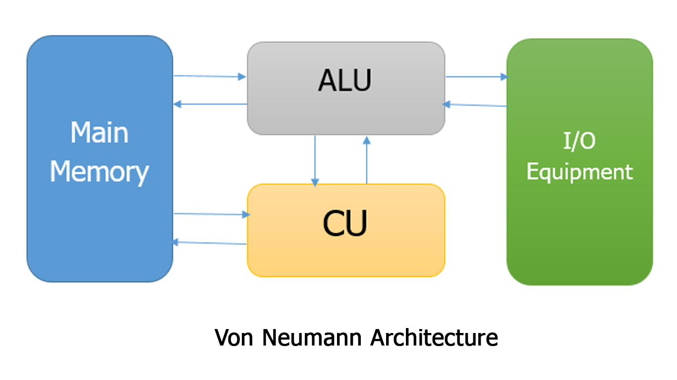
The main memory is used to store data and instructions. The ALU is capable of performing arithmetic and logical operations on binary data. The program control unit interprets the instructions in memory and causes them to be executed. The I/O unit gets operated from control unit.
The Von Neumann architecture is the fundamental basis for the architecture of today’s digital computers. Thus, it is important to have an idea of internal structure of the CPU and CU of Von Neumann machine.
The memory of Von Neumann machine consists of 1000 storage locations called words, of 40 bits each. Both the data and instructions are stored in it. The CU operates the computer by fetching instructions from the memory and executing them one at a time.
The storage location of CU and ALU are called registers. The various registers of this model are:
- Memory Buffer Register (MBR): It consists of words to be stored in memory or is used to receive a word from the memory.
- Memory Address Register (MAR): It contains the address in memory of the word to be written from or read into MBR.
- Instruction Register (IR): It contains 8 bit opcode being executed.
- IBR (Instruction Buffer Register): It is used to temporarily hold the instructions from word in memory.
- Program Counter (PC): It contains the address of the next instruction to be fetched from the memory.
- The accumulator (A) and the multiplier quotient (MQ) are employed to temporarily hold the operands and the result of ALU operations.
In Von Neumann architecture, the same memory is used for storing instructions and data. Similarly, a single bus, either data bus or address buss is used for reading data and instructions from or writing data and instruction to the memory.
Later, it was revealed that this feature of Von Neumann architecture limited the processing speed of the computer. So, to improve the processing speed of computer, Harvard architecture was introduced.
-
Harvard Architecture: The Harvard architecture consists of separate memory locations for the programs and data. Each memory space has its own address and data bus. As a result of this, both the instructions, and data can be fetched from the memory concurrently. Thus, a significant processing speed is observed over Von Neumann type architecture.

From the figure, we can see that there are two data and two address buses for the program and data memory space separately. The program memory data bus and data memory bus are multiplexed to form single data bus whereas program memory address bus and data memory address bus are multiplexed to form a single address bus. Hence, there are two blocks of RAM chip, one for program memory and the other for data memory space. The data memory address arithmetic unit generates the data memory address. The data memory address bus carries the memory address of the data whereas the program memory address bus carries the memory address of the instruction. There is central arithmetic logic unit which consists of ALU, multiplier, accumulator and scaling chief register. The program counter is used to address program memory. The contents are updated following each decode operation. The control unit controls the sequence of operations to be executed. The data and control bus are bidirectional whereas the address bus is unidirectional.


